
포지션 상세
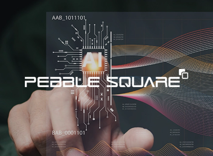
페블스퀘어는 PIM아키텍처를 기반으로 AI 반도체 설계와 AI 솔루션을 개발하는 팹리스 기업입니다. 폰 노이만(Von Neumann)구조의 한계를 극복하기 위해 고성능/초저전력의 PIM기반 AI 반도체를 성공적으로 양산하고, 멀티 코어 AI 반도체를 개발하여 국내외에서 실증 중이며 AI 반도체 상용화와 활용 촉진을 위해 다양한 AI 솔루션을 개발 중입니다.
We are seeking a highly skilled and self-motivated Analog and Mixed-Signal Design Engineer to join our advanced IC design team. In this role, you will be responsible for designing, simulating, and driving the characterization of high-performance analog and mixed-signal blocks—with a strong focus on high-speed, low-power, and low-noise ADC/DAC architectures.
You will own the entire design cycle from architectural definition and transistor-level design to physical layout verification and silicon characterization, ensuring the highest level of analog computing in memory performance.
Design the architecture, transistor-level design, and simulation of high-performance data converters (e.g., SAR ADCs, Single-Slope ADCs and high-speed DACs/Ramp Generators) for analog computing in memory readout circuits.
• Block-Level Design:
Design and optimize critical analog blocks including ADC, ADC calibration scheme, DAC, OP-amplifiers, Bandgap References (BGR), and high-speed comparators.
• Layout & Verification:
Oversee and produce high-quality custom IC layouts from schematic to chip-level, utilizing advanced matching techniques and mitigating parasitic effects.
• Advanced Simulation:
Perform rigorous circuit noise analysis, mismatch/Monte Carlo simulations, and fast-Spice simulations for large-scale analog/mixed-signal blocks.
• Silicon Characterization:
Drive post-silicon characterization, debug, and optimization to ensure the analog computing in memory achieves peak performance metrics (SNR, High sampling speed)
• Documentation & Collaboration:
Plan, execute, and thoroughly document design specifications and verification results with limited supervision, collaborating closely with digital design.
5+ years of proven hands-on experience in analog/mixed-signal IC design (experience in memory chip is plus).
• Data Converter Knowledge:
Strong background in ADC/DAC design topologies.
• EDA Tools Proficiency:
Extensive experience with industry-standard EDA/CAD tools, including Cadence Design Framework (Virtuoso, Spectre/APS), Mentor Graphics Calibre (DRC/LVS/PEX), and fast-Spice simulators (XA, FineSim, or NanoTime).
• Layout Skills:
Expert knowledge of full-custom physical layout, device matching methodologies, and deep sub-micron parasitic effects.
• Education:
BSEE or equivalent required; MSEE or Ph.D. with a focus on Analog/Mixed-Signal IC design is strongly preferred.
• Soft Skills:
Excellent communication, cross-functional teamwork, and a passion for cutting-edge imaging technologies.
* All application documents, including your resume, must be submitted in English.
We are seeking a highly skilled and self-motivated Analog and Mixed-Signal Design Engineer to join our advanced IC design team. In this role, you will be responsible for designing, simulating, and driving the characterization of high-performance analog and mixed-signal blocks—with a strong focus on high-speed, low-power, and low-noise ADC/DAC architectures.
You will own the entire design cycle from architectural definition and transistor-level design to physical layout verification and silicon characterization, ensuring the highest level of analog computing in memory performance.
주요업무
• Analog/Mixed-Signal Design:Design the architecture, transistor-level design, and simulation of high-performance data converters (e.g., SAR ADCs, Single-Slope ADCs and high-speed DACs/Ramp Generators) for analog computing in memory readout circuits.
• Block-Level Design:
Design and optimize critical analog blocks including ADC, ADC calibration scheme, DAC, OP-amplifiers, Bandgap References (BGR), and high-speed comparators.
• Layout & Verification:
Oversee and produce high-quality custom IC layouts from schematic to chip-level, utilizing advanced matching techniques and mitigating parasitic effects.
• Advanced Simulation:
Perform rigorous circuit noise analysis, mismatch/Monte Carlo simulations, and fast-Spice simulations for large-scale analog/mixed-signal blocks.
• Silicon Characterization:
Drive post-silicon characterization, debug, and optimization to ensure the analog computing in memory achieves peak performance metrics (SNR, High sampling speed)
• Documentation & Collaboration:
Plan, execute, and thoroughly document design specifications and verification results with limited supervision, collaborating closely with digital design.
자격요건
• Experience:5+ years of proven hands-on experience in analog/mixed-signal IC design (experience in memory chip is plus).
• Data Converter Knowledge:
Strong background in ADC/DAC design topologies.
• EDA Tools Proficiency:
Extensive experience with industry-standard EDA/CAD tools, including Cadence Design Framework (Virtuoso, Spectre/APS), Mentor Graphics Calibre (DRC/LVS/PEX), and fast-Spice simulators (XA, FineSim, or NanoTime).
• Layout Skills:
Expert knowledge of full-custom physical layout, device matching methodologies, and deep sub-micron parasitic effects.
• Education:
BSEE or equivalent required; MSEE or Ph.D. with a focus on Analog/Mixed-Signal IC design is strongly preferred.
• Soft Skills:
Excellent communication, cross-functional teamwork, and a passion for cutting-edge imaging technologies.
* All application documents, including your resume, must be submitted in English.
